
C8051F000/1/2/5/6/7 and C8051F010/1/2/5/6/7 are mixed-signal 32KB ISP flash MCU products produced by CYGNAL. They have SAR ADC, 12-bit DAC, temperature sensor, voltage comparators and other analog peripherals, as well as 21 interrupts, 8051 CPU (25MIPS), JTAG debug circuit and other digital peripherals.
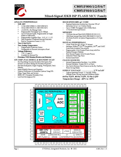
The C8051F000/1/2/5/6/7 and C8051F010/1/2/5/6/7 devices are fully integrated mixed‑signal System‑on‑Chip microcontrollers. Each part includes a true 12‑bit (or 10‑bit) multi‑channel ADC, two 12‑bit DACs, voltage comparators, a programmable gain amplifier, a voltage reference, and an 8051‑compatible core with up to 32 KB flash memory. On‑chip peripherals such as SMBus/I²C, SPI, UART, a programmable counter/timer array, and four 16‑bit timers are available, and JTAG/IEEE‑1149.1 debug provides non‑intrusive in‑circuit debugging.
The devices operate from 2.7 V to 3.6 V, draw about 12.5 mA at 25 MHz, and are specified for an industrial temperature range of –40 °C to +85 °C. They are offered in 64‑pin TQFP, 48‑pin TQFP and 32‑pin LQFP packages, and support up to 21 vectored interrupt sources and up to 25 MIPS throughput at a 25 MHz clock.
| ADC Resolution | 12‑bit (C8051F000/1/2, C8051F005/6/7); 10‑bit (C8051F010/1/2, C8051F015/6/7) |
|---|---|
| Flash Memory | 32 KB (in‑system programmable, 512‑byte sectors) |
| Internal RAM | 256 B (F000/01/02/10/11/12) or 2304 B (F005/06/07/15/16/17) |
| Supply Voltage | 2.7 V to 3.6 V |
| Operating Current | Typical 12.5 mA @ 25 MHz |
| Temperature Range | -40 °C to +85 °C |
| Interrupt Sources | 21 vectored interrupt sources |
| Maximum MIPS | Up to 25 MIPS at 25 MHz |
| Package Options | 64‑Pin TQFP, 48‑Pin TQFP, 32‑Pin LQFP |
They operate from 2.7 V to 3.6 V.
The devices provide 21 vectored interrupt sources.
Up to 25 MIPS can be achieved with a 25 MHz clock.
Yes, it has IEEE‑1149.1 compliant JTAG debug and boundary‑scan support.