
This document introduces the CYGNAL Integrated Products, Inc. C8051F206, C8051F220/1/6, and C8051F230/1/6 mixed-signal 8KB ISP FLASH MCU family. The product features JTAG interface, 8K x 8 ISP FLASH, 1280 x 8 SRAM, SAR ADC, clock circuit, PGA, AMUX, voltage comparators, analog peripherals, digital I/O, timers, high-speed controller core emulation circuitry, 22 interrupts, 8051 CPU, internal data RAM, XRAM, and FLASH.
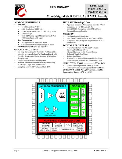
The C8051F2xx family is a mixed‑signal System‑on‑Chip MCU line featuring an 8051‑compatible core, on‑chip flash, SRAM, and optional ADCs. Models include the C8051F206 with a 12‑bit SAR ADC, the C8051F220/1/6 with an 8‑bit SAR ADC, and the C8051F230/1/6 without an ADC. All devices operate from 2.7 V to 3.6 V and are supplied in 48‑pin TQFP or 32‑pin LQFP packages.
The manual provides detailed descriptions of the CPU core, memory map, digital and analog peripherals, clocking options, JTAG debug interface, and power‑management modes. It also includes register tables, timing diagrams, and programming guidelines for flash and peripheral configuration.
| Supply Voltage | 2.7 V to 3.6 V |
|---|---|
| Typical Operating Current | 10 mA @ 25 MHz |
| Temperature Range | -40 °C to +85 °C |
| Flash Memory Size | 8 KB (8 k Bytes) |
| Internal SRAM | 256 Bytes |
| Additional XRAM (selected models) | 1024 Bytes |
| Maximum Clock Frequency | 25 MHz |
| ADC Resolution | 8‑bit (C8051F220/1/6) / 12‑bit (C8051F206) |
| ADC Sample Rate | Up to 100 ksps |
| Package Options | 48‑pin TQFP and 32‑pin LQFP |
The device operates from 2.7 V to 3.6 V.
They are rated for -40 °C to +85 °C operation.
Each device includes 8 KB of in‑system programmable flash memory.