
This document describes the features and characteristics of the N-Channel Enhancement Mode Field Effect Transistor CEDF634/CEUF634, including maximum operating voltage, maximum operating current, and on-resistance. The product features a super high dense cell design for extremely low on-resistance and high power and current handling capability.
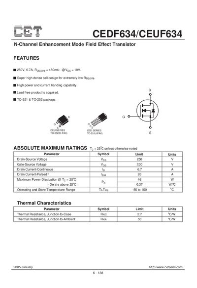
The CEDF634/CEUF634 is an N‑Channel enhancement mode field‑effect transistor offered in TO‑252 (D‑PAK) and TO‑251 (S‑PAK) packages. It features a high drain‑source voltage of 250 V, a continuous drain current of 6.7 A, and a pulsed current capability of 26 A, making it suitable for high‑power applications.
The datasheet lists detailed electrical characteristics, absolute maximum ratings, and thermal parameters such as junction‑to‑case resistance of 27 °C·W and junction‑to‑ambient resistance of 50 °C·W. It also includes dynamic and switching characteristics, capacitance values, and typical performance graphs.
| Drain‑Source Voltage (VDS) | 250 V |
|---|---|
| Gate‑Source Voltage (VGS) | +30 V |
| Continuous Drain Current (ID) | 6.7 A |
| Pulsed Drain Current (ID,pulse) | 26 A |
| Maximum Power Dissipation | 46 W |
| Junction‑to‑Case Thermal Resistance (RJC) | 27 °C·W |
| Junction‑to‑Ambient Thermal Resistance (RJA) | 50 °C·W |
| Input Capacitance (Ciss) | 630 pF |
| Output Capacitance (Coss) | 100 pF |
| Turn‑On Delay Time (t_on) | 19 ns |
The device is rated for a maximum drain‑source voltage of 250 V.
The continuous drain current is specified as 6.7 A.
It is offered in TO‑252 (D‑PAK) and TO‑251 (S‑PAK) packages.
The device can operate from –55 °C to 150 °C.