
The MAX9152 is a 2 x 2 crosspoint switch designed for applications requiring high speed, low power, and low-noise signal distribution. This device includes two LVDS/LVPECL inputs, two LVDS outputs, and two logic inputs that set the internal connections between differ- ential inputs and outputs. The MAX9152 can be programmed to connect any input to either or both outputs, allowing it to be used in the following configurations: 2 ✕ 2 crosspoint switch, 2:1 mux, 1:2 demux, 1:2 splitter, or dual repeater. This flexi- bility makes the MAX9152 ideal for protection switching in fault-tolerant systems, loopback switching for diag- nostics, fanout buffering for clock/data distribution, and signal regeneration for communication over extended distances. Ultra-low 120psPK-PK (max) PRBS jitter ensures reliable communications in high-speed links that are highly sen- sitive to timing error, especially those incorporating clock-and-data recovery, or serializers and deserializ- ers. The high-speed switching performance guarantees an 800Mbps data rate and less than 50ps (max) skew between channels. LVDS inputs and outputs are compatible with the TIA/EIA-644 LVDS standard. The LVDS inputs are designed to also accept LVPECL signals directly, and PECL signals with an attenuation network. The LVDS outputs are designed to drive 75Ω or 100Ω loads, and feature a selectable differential output resistance to minimize reflections. The MAX9152 is available in 16-pin TSSOP and SO packag
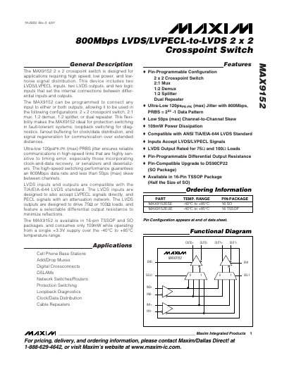
The MAX9152 2 × 2 crosspoint switch provides flexible routing of high‑speed differential signals. It can be programmed as a 2:1 mux, 1:2 demux, 1:2 splitter, or dual repeater, making it suitable for protection switching, loopback diagnostics, clock/data distribution and signal regeneration.
Electrical characteristics include a single‑supply operation from +3.0 V to +3.6 V, 109 mW power dissipation at +3.3 V, and operation over –40 °C to +85 °C. The device supports LVDS‑standard loads of 75 Ω or 100 Ω, offers selectable differential output resistance, and is offered in 16‑pin TSSOP and SO packages.
| Maximum data rate | 800 Mbps |
|---|---|
| Channel‑to‑channel skew (max) | 50 ps |
| Jitter (PK‑PK, max) | 120 ps |
| Power dissipation | 109 mW |
| Supply voltage range | +3.0 V to +3.6 V |
| Operating temperature range | -40 °C to +85 °C |
| LVDS output load rating | 75 Ω or 100 Ω |
| Package types | 16‑pin TSSOP, 16‑pin SO |
The MAX9152 supports a maximum data rate of 800 Mbps.
It operates from a supply voltage of +3.0 V to +3.6 V.
The device consumes only 109 mW when powered at +3.3 V.
The LVDS outputs can drive either 75 Ω or 100 Ω loads.