
SN74LVC08A-Q1 is a quadruple 2-input positive-AND gate designed by Texas Instruments. It operates from 2.7-3.6V and can drive 3.3V or 5V devices.
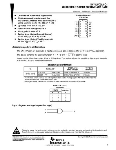
The SN74LVC08A-Q1 is a quadruple 2‑input positive‑AND gate designed for operation from 1.65 V to 3.6 V (typical) and accepts input voltages up to 5.5 V, making it suitable for mixed‑voltage systems. It offers a maximum propagation delay of 4.1 ns at 3.3 V and includes ESD protection exceeding 2000 V.
The device is offered in SOIC‑D and TSSOP‑PW packages, with ordering codes SN74LVC08AQD and SN74LVC08AQPW. Mechanical drawings, land‑pattern data, and thermal information are provided, and the latest package options can be found on the TI website.
| Operating supply voltage | 1.65 V to 3.6 V |
|---|---|
| Maximum input voltage | 5.5 V |
| Maximum propagation delay (tpg) | 4.1 ns at 3.3 V |
It operates from 1.65 V to 3.6 V, with a typical range of 2.7 V to 3.6 V for recommended conditions.
The maximum propagation delay is 4.1 ns at a supply voltage of 3.3 V.