
This data sheet provides detailed information on SN74ALVC08 quadruple 2-input positive-AND gate characteristics including operating voltage range, maximum propagation delay, output drive current, latch-up performance, ESD protection, etc.
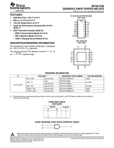
The SN74ALVC08 is a quadruple 2‑input positive‑AND gate designed for operation from 1.65 V to 3.6 V. It offers a maximum propagation delay of 2.9 ns at 3.3 V and can source up to +24 mA output drive at 3.3 V. The device complies with JESD‑22 ESD protection standards and includes latch‑up performance exceeding 250 mA per gate.
The datasheet lists ordering numbers for multiple package options (QFN‑RGY, SOIC‑D, TSSOP‑PW, etc.), provides absolute‑maximum and recommended operating conditions, electrical characteristics, and packaging material specifications. An important notice at the end covers warranty, availability, and safety‑critical usage restrictions.
| Supply voltage range | 1.65 V to 3.6 V |
|---|---|
| Maximum output drive current | +24 mA at 3.3 V |
| Maximum propagation delay | 2.9 ns at 3.3 V |
| Continuous output current | +50 mA |
| Operating temperature range | -40 °C to 85 °C |
| Storage temperature range | -65 °C to 150 °C |
The device operates from 1.65 V to 3.6 V.
It can source up to +24 mA output drive at 3.3 V.
The recommended free‑air operating temperature is –40 °C to 85 °C.