
CD4011UB is a dual input four-input NAND gate from TI. It is low power, high speed and high reliability. It is available in 14-pin hermetic dual-in-line ceramic (F3A suffix), 14-lead dual-in-line plastic (E suffix), 14-lead small-outline packages (M, MT, M96, and NSR suffixes), and 14-lead thin shrink small-outline packages (PW and PWR suffixes).
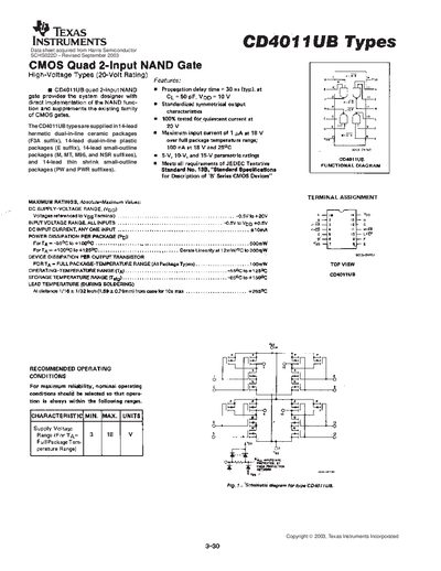
The CD4011UB is a CMOS quad 2‑input NAND gate available in high‑voltage (20 V) versions. The datasheet describes its functional features, typical propagation delay of 30 ns, input capacitance of 50 pF, and low quiescent current, making it suitable for a wide range of digital logic applications.
Technical sections cover static and dynamic electrical characteristics, recommended operating conditions, mechanical dimensions, and detailed package options (PDIP, SOIC, TSSOP, etc.). Ordering information, RoHS compliance, and an important notice about product warranties and usage restrictions are also included.
| Propagation delay time (typ) | 30 ns |
|---|---|
| Supply voltage range | -0.5 V to +20 V |
The typical propagation delay time is 30 ns.
The device operates from –0.5 V up to +20 V.