
This data sheet details the features of the CD54HC30/CD54HCT30 8-input NAND gate.
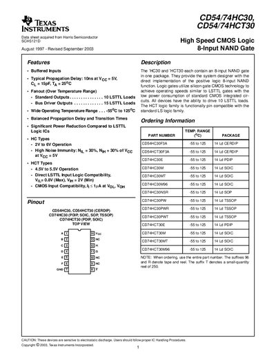
The CD54/74HC30 and CD54/74HCT30 devices integrate an 8‑input NAND gate in a single package. They provide high‑speed CMOS logic with buffered inputs, low power consumption, and the ability to drive standard LSTTL loads. The HCT family is pin‑compatible with LS logic and supports direct LSTTL input compatibility.
The document includes functional diagrams, pinout tables, absolute maximum ratings, DC electrical specifications, switching characteristics, mechanical dimensions, and a comprehensive package option addendum with ordering details and RoHS status.
| Typical Propagation Delay | 10 ns |
|---|---|
| Fanout (Standard Outputs) | 10 LSTTL Loads |
| Fanout (Bus Driver Outputs) | 15 LSTTL Loads |
| Operating Temperature Range | -55°C to 125°C |
| Supply Voltage (HC Types) | 2 V to 6 V |
| Supply Voltage (HCT Types) | 4.5 V to 5.5 V |
The typical propagation delay is 10 ns at VCC = 5 V, CL = 15 pF, and a temperature of 25 °C.
It operates from –55 °C up to 125 °C.
Standard outputs can drive up to 10 LSTTL loads.