
SN54HCT08 and SN74HCT08 are four independent 2-input AND gates that perform the Boolean function Y = A • B or Y = A • B in positive logic. They operate in a voltage range of 4.5 V to 5.5 V and have an output current of ±4 mA and an input current of 1 µA. The package forms are PDIP-N, SOIC-D, SOIC-D, DIP-N, SOP-NS, SSOP-DB, TSSOP-PW, TSSOP-PW, CDIP-J, and CFP-W.
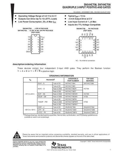
The SN54HCT08 and SN74HCT08 are CMOS logic devices that contain four independent 2‑input positive‑AND gates. The gates operate with TTL‑compatible input levels and provide standard logic functionality.
Typical operating conditions include a supply voltage of 4.5 V to 5.5 V, low input current (1 µA max), and low power consumption (20 µA max ICC). Output drive can source up to ten LSTTL loads, with a typical propagation delay of about 13 ns. The devices are offered in a variety of packages such as PDIP, SOIC, SSOP, and TSSOP, each with specified thermal impedance and mechanical dimensions.
| Supply voltage range | 4.5 V to 5.5 V |
|---|---|
| Output drive capability | Up to 10 LSTTL loads |
| Power consumption (ICC) | 20 µA max |
| Typical propagation delay (tpd) | 13 ns |
| Input low current | 1 µA max |
| High‑level input voltage (VIH) | 4.5 V to 5.5 V |
| Package thermal impedance (θJA) – D package | 86 °C/W |
The devices are specified to operate from 4.5 V to 5.5 V supply voltage.
Each device contains four independent 2‑input positive‑AND gates.
The typical propagation delay is about 13 ns.
Available packages include PDIP, SOIC, SSOP, and TSSOP in various density options.