
This document mainly introduces the product's features and characteristics, including 2-V to 5.5-V VCC operation, max tpd of 7ns at 5V, typical VOLP (Output Ground Bounce) less than 0.8V at VCC=3.3V, typical VOHV (Output VOH Undershoot) greater than 2.3V at VCC=3.3V, support all ports of mixed-mode voltage operation, Ioff support partial-power-down mode operation, latch-up performance exceeds 100mA per JESD 78, class II, ESD protection exceeds JESD 22 - 2000-V Human-Body Model (A114-A) - 200-V Machine Model (A115-A) - 1000-V Charged-Device Model (C101) etc.
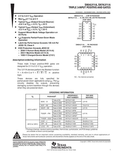
The SN74LV11A (also marked SN54LV11A) is a CMOS triple 3‑input positive‑AND gate designed for 2 V to 5.5 V supply operation. It implements the Boolean function Y = A·B·C and includes features such as partial‑power‑down mode, latch‑up protection, and robust ESD protection meeting JESD‑22 standards.
The device is offered in multiple surface‑mount packages (SOIC‑D, SSOP‑DB, TSSOP‑PW, etc.) with detailed ordering information, thermal impedance data, and mechanical dimensions provided in the package addendum. Texas Instruments supplies full packaging, handling, and reliability data on its website.
| ESD protection (Human‑Body Model) | 2000 V |
|---|