
This document describes the features and characteristics of the SN54AC00 and SN74AC00 products. They are four independent 2-input NAND gates, and each gate performs the Boolean function of Y = A × B or Y = A + B in positive logic. These products are designed for 2V to 6V voltage operation, accept voltages up to 6V, and have a maximum propagation delay of 7ns.
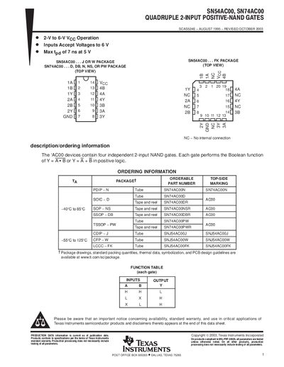
The SN54AC00 and SN74AC00 families are quadruple 2‑input positive‑NAND gates that operate with supply voltages from 2 V to 6 V. Each gate implements the Boolean function Y = A·B in positive logic and is offered in a variety of packages such as PDIP, SOIC, SSOP, TSSOP and CFP.
The document provides absolute‑maximum ratings, recommended operating conditions, electrical characteristics, ordering information, package option addenda, mechanical drawings and packaging material specifications. It also includes the standard TI important notice and RoHS‑compliant packaging details.
| Maximum propagation delay | 7 ns at 5 V |
|---|
The maximum propagation delay is 7 ns when powered at 5 V.