
The document introduces three flash memory products, including K9F5608R0DK9F5608D0D, K9F5608U0D, and K9F5608X0D. The document mentions the specifications and characteristics of these three products and states that they are subject to change. Additionally, the document emphasizes that these products are not intended for use in life support, medical, and military applications.
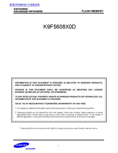
The K9F5608X0D is a 256‑Mbit NAND flash memory offered in 1.8 V, 2.65 V and 3.3 V versions, suitable for solid‑state storage and portable applications. The datasheet provides detailed electrical characteristics, pin descriptions, package options, and functional block diagrams.
Key features include a typical program time of 200 µs, block erase time of 2 ms, endurance of 100 k program/erase cycles, and data retention of 10 years. Various package types such as 63‑ball FBGA and TSOP1 are listed with their dimensions and voltage ranges.
| Memory density | 256 Mbit + 8 Mbit spare |
|---|---|
| Organization | (32M + 1024K) bit × 8 bit |
| Page size | 528 bytes (512 + 16) |
| Block size | 16 KB + 512 B |
| Typical program time | 200 µs (typ.) |
| Typical block erase time | 2 ms (typ.) |
| Endurance | 100 k program/erase cycles |
| Data retention | 10 years |
| Supply voltage (1.8 V device) | 1.65 ~ 1.95 V |
| Package (FBGA) | 63‑ball FBGA, 9 × 11 mm, 0.8 mm pitch |
The typical program time is 200 µs.
It is rated for 100 k program/erase cycles.
The 1.8 V device operates from 1.65 V to 1.95 V.
Each page is 528 bytes (512 + 16 bytes).