
This document is the errata of 512Mb/256Mb 1.8V NAND Flash released by Samsung Electronics, Korea. It contains some AC characteristics not meeting the specification, improvement schedule and workaround.
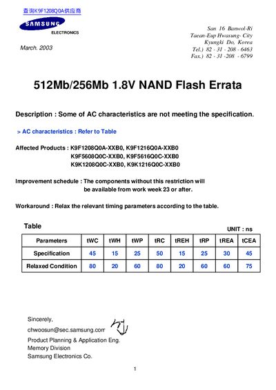
This datasheet provides errata information, specifications, and electrical characteristics for Samsung's K9F56XXQ0C (1.8 V) and K9F56XXU0C (3.3 V) NAND flash memory devices. It lists affected product part numbers, the nature of the AC‑characteristic deviation, and the recommended workaround of relaxing timing parameters.
The document also contains detailed functional block diagrams, pin configurations, package dimensions, command sets, and timing tables (tWC, tWH, tWP, etc.). Additional specifications such as voltage ranges, memory organization, endurance, and data‑retention are included for design engineers and service technicians.
| Voltage supply (1.8 V device) | 1.70 V ~ 1.95 V |
|---|---|
| Memory organization | 32 M × 8 bit (256 Mbit) or 16 M × 16 bit (256 Mbit) |
| Package type (TSOP1) | 48‑Pin lead‑free plastic TSOP I (12 × 20 / 0.5 mm pitch) |
| Endurance | 100 K program/erase cycles |
| Data retention | 10 years |
The errata applies to K9F1208Q0A‑XXB0, K9F1216Q0A‑XXB0, K9F5608Q0C‑XXB0, K9F5616Q0C‑XXB0, K9K1208Q0C‑XXB0, and K9K1216Q0C‑XXB0 devices.
Relax the relevant timing parameters according to the provided timing table.
The minimum Vcc for the 1.8 V devices is now 1.70 V.