
The GS88237BB/D is a 9Mb SCD/DCD synchronous burst SRAM with a storage capacity of 256K x 36. It operates at frequencies ranging from 333 MHz to 200 MHz and supports voltage supplies of 2.5 V or 3.3 V. It features single/dual cycle deselect, IEEE 1149.1-compatible boundary scan, selectable high/low output drive mode, linear or interleaved burst mode, automatic power-down, and more.
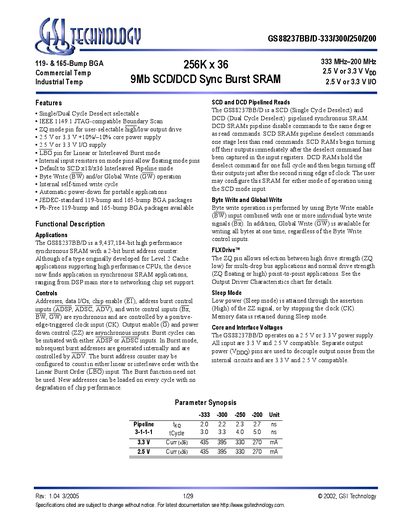
The GS88237BB/D series is a 9,437,184‑bit high‑performance synchronous SRAM offered in 256K × 36 organization. It supports both Single Cycle Deselect (SCD) and Dual Cycle Deselect (DCD) pipelined reads, with selectable core voltages of 2.5 V or 3.3 V and speed grades of 333 MHz, 300 MHz, 250 MHz, and 200 MHz. The device is available in 119‑bump and 165‑bump BGA packages, including Pb‑free options.
Typical applications include Level‑2 cache, DSP main store, and networking chip‑set support where high‑performance burst access is required. Ordering information provides part numbers for each speed grade and package, and the datasheet includes pin descriptions, mode functions, burst counter sequences, and timing diagrams to aid system integration.
| Capacity | 9,437,184 bits (9 Mb) |
|---|---|
| Organization | 256K × 36 |
| Speed grades | 333 MHz, 300 MHz, 250 MHz, 200 MHz |
| Core voltage | 2.5 V or 3.3 V (±10%) |
| Package types | 119‑bump BGA, 165‑bump BGA (Pb‑free available) |
| ZQ pin function | Selects high‑drive or low‑drive output strength |
| LBO pin function | Selects linear or interleaved burst order |
It operates from either a 2.5 V or a 3.3 V core supply, with a ±10 % tolerance.
The device is offered in 119‑bump BGA and 165‑bump BGA packages, both available in Pb‑free versions.
The LBO pin selects linear burst order or interleaved burst order; the default is interleaved pipeline mode.
The ZQ pin selects between high‑drive (low impedance) and low‑drive (high impedance) output strength.