
This datasheet is for GS88237BB/D-xxxV 256K x 36 9Mb SCD/DCD Sync Burst SRAM. It provides the main features of the product, such as operating voltage, operating temperature, and package type.
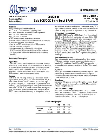
The GS88237BB/D-xxxV is a 9,437,184‑bit high‑performance synchronous SRAM offered in 119‑bump and 165‑bump BGA packages. It supports both single‑cycle (SCD) and dual‑cycle (DCD) pipelined operation, with selectable 1.8 V or 2.5 V core and I/O supplies.
The document provides a full functional description, pin definitions, mode‑pin functions, burst‑counter sequences, and ordering information for various speed‑grade and temperature‑range options.
| Capacity | 256K x 36 |
|---|---|
| Core voltage | 1.8 V or 2.5 V |
| I/O voltage | 1.8 V or 2.5 V |
| Package options | 119‑bump BGA, 165‑bump BGA |
| Maximum speed | 250 MHz (typical) |
| Current consumption (typical) | 330 mA |
It operates on a 1.8 V or 2.5 V power supply.
The device is offered in 119‑bump and 165‑bump BGA packages.
Sleep mode is entered by asserting the ZZ signal high or by stopping the clock.
Speed grades of 200 MHz and 250 MHz are offered.