
The GS882ZV18/36B is a 9Mb Synchronous Static SRAM. GSI's NBT SRAMs, like ZBT, NtRAM, NoBL or other pipelined read/double late write or flow through read/single late write SRAMs, allow utilization of all available chip selects, thereby achieving zero wait read-write-read bus utilization. The product is powered by 1.8V VDD and 1.8V I/O, features a user-configurable pipeline and flow-through mode, ZQ mode pin, IEEE 1149.1 JTAG-compatible Boundary Scan, on-chip parity encoding and error detection, LBO pin for linear or interleave burst mode, pin-compatibility with 2M, 4M, and 18M devices, byte write operation (9-bit Bytes), 3 chip enable signals for easy depth expansion, ZZ pin for automatic power-down, JEDEC-standard 119-bump BGA and 165-bump FPBGA packages, lead-free 119-bump and 165-bump BGA packages available.
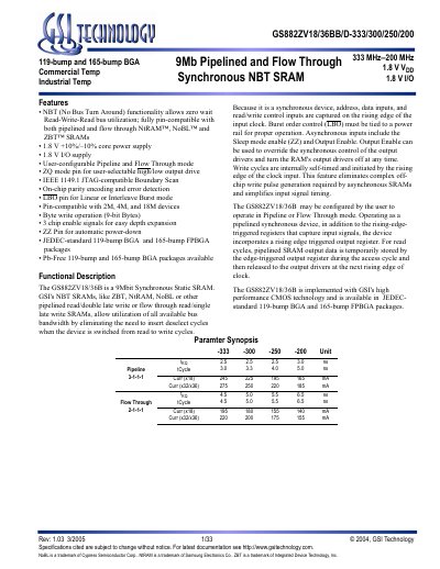
The GS882ZV18/36BB/D series is a 9 Mbit synchronous static RAM that implements No Bus Turn Around (NBT) functionality, allowing zero‑wait read‑write‑read bus utilization. It operates from a 1.8 V core and I/O supply, supports frequencies from 333 MHz down to 200 MHz, and is available in 119‑bump and 165‑bump BGA packages for both 18‑bit and 36‑bit data widths. The device offers configurable pipeline or flow‑through modes, on‑chip parity, JTAG boundary‑scan, and optional linear or interleaved burst ordering.
Functional details include separate clock, chip‑enable, write‑enable, and byte‑write signals, as well as a ZZ pin for entering a low‑power sleep mode. The SRAM includes a burst address counter, ZQ pin for drive‑strength selection, and supports both commercial and industrial temperature ranges. Ordering information lists specific part numbers for each speed and package variant.
| Capacity | 9 Mbit |
|---|---|
| Operating Frequency | 333 MHz – 200 MHz |
| Core Supply Voltage | 1.8 V ±10% |
| Package Types | 119‑bump BGA and 165‑bump FPBGA |
| Temperature Range | Commercial and Industrial |
NBT (No Bus Turn Around) functionality allows zero‑wait read‑write‑read bus utilization, eliminating turnaround cycles between read and write operations.
Sleep mode is entered by pulling the ZZ pin high; after two clock cycles the device enters a low‑current power‑down state.
The SRAM is offered in 119‑bump BGA and 165‑bump FPBGA packages, each in 18‑pin and 36‑pin configurations.