
The GS88237BB/D-xxxV is a 9,437,184-bit high performance synchronous SRAM with a 2-bit burst address counter, which supports JEDEC-standard 119-bump and 165-bump BGA packages.
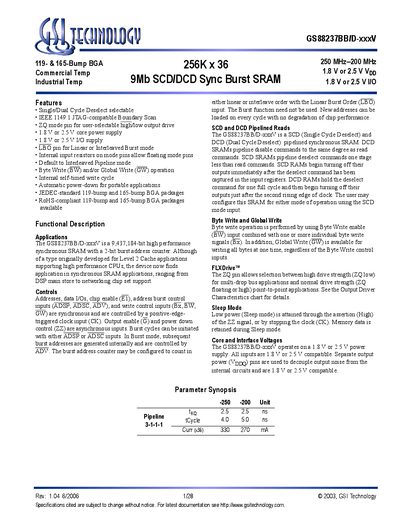
The GS88237BB/D-xxxV is a high‑performance 9,437,184‑bit synchronous SRAM offered in a 256K × 36 configuration. It supports both Single‑Cycle Deselect (SCD) and Dual‑Cycle Deselect (DCD) pipelined modes, with selectable Byte Write and Global Write functions, and provides a ZQ pin for high‑drive or normal‑drive output strength.
Designed for Level‑2 cache, DSP main store, and networking chip‑set applications, the device operates from a 1.8 V or 2.5 V core and I/O supply, includes low‑power sleep mode via the ZZ pin, and is available in JEDEC‑standard 119‑bump and 165‑bump BGA packages. Ordering information and revision history are provided at the end of the datasheet.
| Memory organization | 256K x 36 |
|---|---|
| Total capacity | 9,437,184 bits (9 Mb) |
| Core voltage | 1.8 V or 2.5 V |
| I/O voltage | 1.8 V or 2.5 V |
| Maximum operating frequency | 250 MHz‑200 MHz |
| Package types | 119‑bump BGA, 165‑bump BGA |
| Temperature range | Commercial and Industrial |
It operates on a 1.8 V or 2.5 V core supply, and all inputs are compatible with 1.8 V or 2.5 V I/O levels.
The device is offered in JEDEC‑standard 119‑bump and 165‑bump BGA packages.
Sleep mode is entered by asserting the ZZ signal high or by stopping the clock.
It supports Byte Write (BW) and Global Write (GW) operations for writing individual or all bytes.