
This document describes the features and characteristics of Fujitsu Semiconductor's flash memory storage product, including the use of 0.23μm process technology, support for simultaneous read/write operations, single 3.0V power supply, compatibility with JEDEC standard commands, and worldwide pinout compatibility.
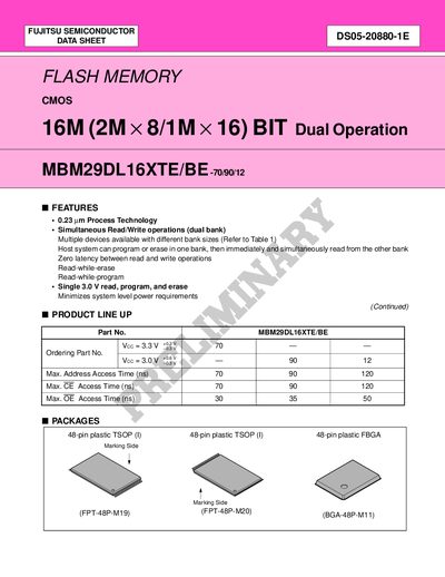
The MBM29DL16XTE/BE series are 16‑Mbit, 3.0 V‑only flash memory devices offered in 48‑pin TSOP(I) and 48‑ball FBGA packages. They feature dual‑bank architecture with simultaneous read/write capability, sliding bank size options, and a minimum of 100 k program/erase cycles.
Key features include single‑voltage operation, fast access times (70 ns‑120 ns), sector‑erase architecture, built‑in protection pins, and automatic low‑power sleep mode. The datasheet provides full pin‑out tables, timing diagrams, and command set compatibility with JEDEC‑standard E7PROMs.
| Process Technology | 0.23 µm |
|---|---|
| Operating Voltage | 3.0 V (single supply) |
| Memory Capacity | 16 Mbit (2 M × 8 / 1 M × 16) |
| Maximum Address Access Time | 70 ns / 90 ns / 120 ns |
| Maximum CE Access Time | 70 ns / 90 ns / 120 ns |
| Maximum OE Access Time | 30 ns / 35 ns / 50 ns |
| Program/Erase Cycle Endurance | ≥ 100 000 cycles |
| Sector Architecture | Eight 4 KB word & thirty‑one 32 KB word sectors (word mode) |
| Low‑Vcc Write Inhibit | < 2.5 V |
The devices are available with maximum address access times of 70 ns, 90 ns, or 120 ns depending on the part.
Each device is rated for a minimum of 100 000 program/erase cycles.
The memory operates from a single 3.0 V supply for read, program, and erase operations.