
This data sheet provides information on the features, applications, pinout, voltage, usage, programming cycles, peripherals, etc. of Altera EPCS1 and EPCS4 devices.
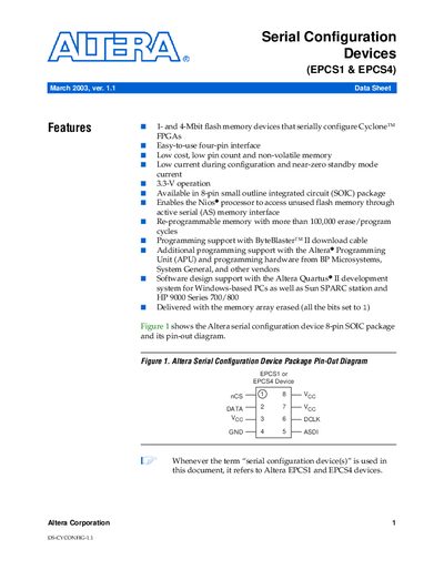
The EPCS1 and EPCS4 devices are 1‑ and 4‑Mbit flash memory parts that serially configure Cyclone™ FPGAs. They feature a low‑cost four‑pin interface, 3.3‑V operation, and an 8‑pin SOIC package. The devices support up to 100,000 erase/program cycles and can be accessed by the Nios® processor via the active‑serial (AS) memory interface.
The datasheet details pin functions, programming methods (ByteBlaster™ II, Altera Programming Unit, third‑party adapters), and timing parameters for both write and read operations. Ordering codes, mechanical dimensions, and compatibility notes are also included.
| Memory Size (EPCS1) | 1,048,576 bits |
|---|---|
| Memory Size (EPCS4) | 4,194,304 bits |
| Operating Voltage | 3.3 V |
| Package | 8‑pin SOIC |
| DCLK high time | 25 ns |
| Chip select (ncs) setup time | 10 ns |
| ASDI data setup time | 5 ns before rising edge on DCLK |
Both devices are supplied in an 8‑pin small outline integrated circuit (SOIC) package.
The devices operate at 3.3 V.
No, serial configuration devices cannot be cascaded.