
This data sheet introduces the information of Altera Cyclone FPGA family, including logic element numbers, RAM capacity, I/O standards, clock frequencies, etc.
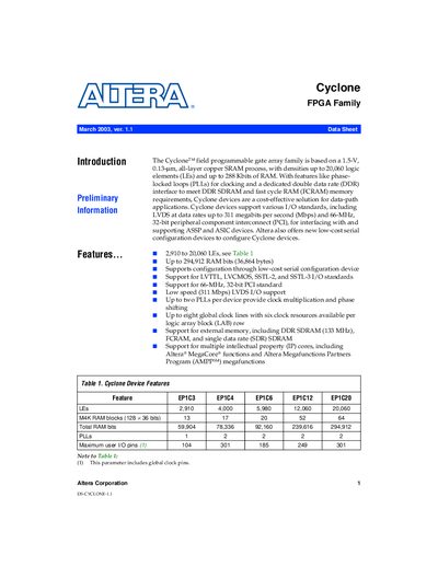
The document describes the Cyclone field programmable gate array (FPGA) family based on a 1.5-V, 0.13-µm SRAM process. Devices in this family range from 2,910 to 20,060 logic elements and support up to 288 Kbits of embedded RAM.
Key features include phase-locked loops (PLLs) for clocking, dedicated double data rate (DDR) interfaces for SDRAM and FCRAM memory, and support for various I/O standards such as LVDS at speeds up to 311 Mbps. The datasheet provides detailed specifications on logic array blocks, global clock networks, power consumption, and available package types including QFP and FineLine BGA.
| Process Technology | 1.5-V, 0.13-µm SRAM process |
|---|---|
| Logic Elements (LEs) | 2,910 to 20,060 |
| Embedded RAM | Up to 288 Kbits |
| LVDS Data Rate | 311 Mbps |
| PCI Support | 66-MHz, 32-bit |
| PLLs per device | Up to two |
Cyclone devices have densities ranging from 2,910 to 20,060 logic elements.
The devices support LVDS at up to 311 Mbps and the 66-MHz, 32-bit PCI standard.
Cyclone devices are supported by the Altera Quartus II design software.