
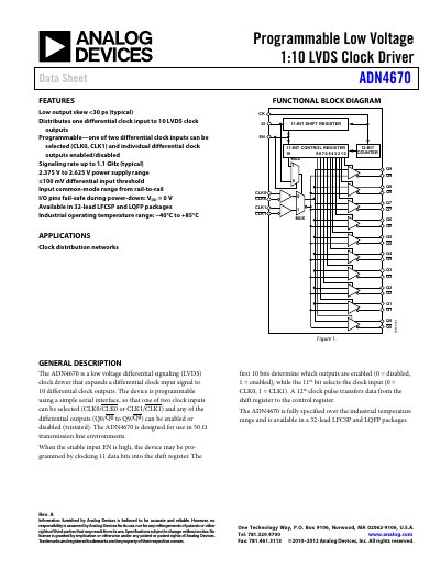
Analog Devices ADN4670 Programmable Low Voltage 1:10 LVDS Clock Driver Data Sheet


Analog Devices ADN4670 Programmable Low Voltage 1:10 LVDS Clock Driver Data Sheet - cover page
Brand
Analog Devices
Category
Other Electronics
Document type
Datasheet
Language
English
Pages
12
File format
PDF
File size
234 KB
Published
03 May, 2012
Updated
29 September, 2023
MD5 checksum
C04575D22320220611D0E68DD9079B9B

About this manual

The ADN4670 is a low‑voltage differential signaling (LVDS) clock driver that distributes a single differential clock input to ten LVDS clock outputs. It features selectable input sources, individual output enable/disable, and fail‑safe operation during power‑down.

The device operates from a 2.375 V to 2.625 V supply, supports up to 1.1 GHz input clock rates, and offers typical output skew under 30 ps. It is offered in 32‑lead LFCSP and LQFP packages and meets industrial temperature specifications (‑40 °C to +85 °C).

What's inside

  • Features
  • Applications
  • Functional Block Diagram
  • General Description
  • Specifications
  • LVDS Switching Characteristics
  • Programming Logic
  • Pin Configuration and Function Descriptions

Specifications

Supply Voltage (VDD)2.375 V to 2.625 V
Low Output Skew<30 ps (typical)
Maximum Input Clock Frequency900 MHz to 1100 MHz
Propagation Delay (Low‑to‑High)2 ns to 3 ns
Output Rise Time (tr)350 ps

Frequently asked questions

What is the supply voltage range for the ADN4670?

The device operates from 2.375 V to 2.625 V.

How many LVDS clock outputs does the ADN4670 provide?

It provides ten differential LVDS clock outputs.

What is the maximum input clock frequency the ADN4670 can handle?

The maximum input frequency is between 900 MHz and 1100 MHz.

What is the typical output skew of the ADN4670?

Typical output skew is less than 30 ps.

Download PDF (234 KB)

More Analog Devices Manuals


View all Analog Devices manuals →