
This document describes the features of International Rectifier's Fifth Generation HEXFET® Power MOSFET PD - 9.1239D. The device has ultra-low on-resistance, dual N-channel, surface mount, and other characteristics, making it suitable for a wide range of applications. It utilizes advanced processing techniques to achieve the lowest possible on-resistance per silicon area. Additionally, it has fast switching speed and rugged design, making it an extremely efficient device. The package has been modified for enhanced thermal characteristics and multiple-die capability, making it ideal for various power applications. With these improvements, multiple devices can be used in an application, significantly reducing board space. The package is compatible with vapor phase, infrared, or wave soldering techniques. Power dissipation greater than 0.8W is achievable in a typical PCB mount application.
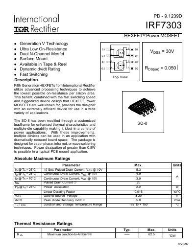
The IRF7303 is a dual‑N‑channel HEXFET power MOSFET offered in a surface‑mount SO‑8 package. It features ultra‑low on‑resistance, fast switching, and a high drain‑to‑source breakdown voltage, making it suitable for a wide range of power applications.
The datasheet provides electrical characteristics, thermal ratings, typical performance curves, and detailed mechanical dimensions, along with packaging information for tape‑and‑reel handling and recommended PCB footprints.
| Drain-to-Source Breakdown Voltage (V(BR)DSS) | 30 V |
|---|---|
| Continuous Drain Current (ID) @ 25°C, VGS=10V | 4.9 A |
| Pulsed Drain Current (ID) @ 25°C, VGS=10V | 5.3 A |
| On‑Resistance (RDS(on)) | 0.050 Ω |
| Maximum Power Dissipation | 2.0 W |
| Gate‑to‑Source Voltage (VGS) | ±20 V |
| Total Gate Charge (Qg) | 25 nC |
| Input Capacitance (Ciss) | 520 pF |
| Output Capacitance (Coss) | 180 pF |
| Junction‑to‑Ambient Thermal Resistance (RθJA) | 62.5 °C/W |
The IRF7303 can withstand up to 30 V drain‑to‑source breakdown voltage.
The on‑resistance is specified as 0.050 Ω.
The device is rated for a maximum power dissipation of 2.0 W.
The total gate charge is 25 nC.