
The Altera ACEX 1K Programmable Logic Device Family is a low cost system-on-a-programmable-chip (SOPC) device that provides high density, high performance, and system-level features.
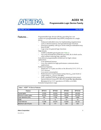
The ACEX 1K family provides low‑cost, high‑density programmable logic with embedded array blocks (EABs) and logic array blocks (LABs). Devices support up to 100 000 gates, 49 152 RAM bits and a wide range of I/O options, making them suitable for communications, DSP and custom logic applications.
The datasheet includes device features, package options from 100‑484 pins, performance tables for common and complex designs, and configuration options such as JTAG, MasterBlaster and ByteBlaster download cables.
| Typical gates | 10,000 to 100,000 |
|---|---|
| Maximum RAM bits | 49,152 bits |
| Package pin count range | 100 to 484 pins |
| Core supply voltage | 2.5 V |
| Global clock signals | Up to six |
An ACEX 1K device can contain up to 49,152 RAM bits.
The core operates with a 2.5‑V internal supply voltage.
The device provides up to six global clock signals.
Typical gate counts range from 10,000 to 100,000 gates.