
BSP318S is a N-Channel Enhancement mode Small-Signal-Transistor with avalanche rated, logic level and dv/dt rated. Product Specification: Drain-Source voltage is 60V, Drain-Source on-state resistance is 0.09 Ohm, Continuous drain current is 2.6A.
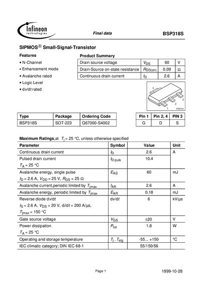
The Infineon BSP318S is an N‑channel SIPMOS small‑signal transistor designed for logic‑level applications. The datasheet provides a complete set of electrical parameters, including drain‑source voltage, continuous and pulsed drain currents, on‑state resistance, gate threshold, and capacitances, as well as thermal ratings and safe‑operating‑area curves.
Key sections cover maximum ratings, thermal characteristics, detailed static and dynamic electrical characteristics, gate‑charge data, reverse‑diode behavior, power‑dissipation limits, and typical output and transfer characteristics. The document also includes mechanical dimensions, package information (SOT‑223), and regulatory notices.
| Drain‑source breakdown voltage (VDS) | 60 V |
|---|---|
| Continuous drain current (ID) | 2.6 A |
| Pulsed drain current (ID(pulse)) | 10.4 A |
| On‑state resistance (RDS(on)) typ | 0.12 Ω |
| On‑state resistance (RDS(on)) max | 0.15 Ω |
| Gate threshold voltage (VGS(th)) typ | 1.2 V |
| Gate charge (Qg) typ | 14 nC |
| Power dissipation (PD) | 1.8 W |
| Thermal resistance, junction‑to‑case (RθJC) | 17 K/W |
| Avalanche energy (EA) | 60 mJ |
| Reverse diode forward voltage (VF) | 0.95 V |
| Input capacitance (Ciss) typ | 300 pF |
| Output capacitance (Coss) typ | 90 pF |
| Reverse recovery time (trr) | 50 ns |
The BSP318S can conduct a continuous drain current of 2.6 A.
The device is rated for a drain‑source breakdown voltage of 60 V.
The typical gate‑threshold voltage is 1.2 V.
The maximum power dissipation is 1.8 W.