
BSP149 is a N-channel, depletion mode, dv /dt rated, Pb-free lead plated small signal transistor. It has maximum ratings of 0.66 A continuous drain current, 0.53 A maximum drain current, 2.6 A pulsed drain current, 6 kV / µs reverse diode dv /dt and 1.8 W maximum power dissipation.
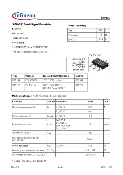
The BSP149 is a small‑signal, N‑channel depletion‑mode MOSFET offered in a PG‑SOT‑223 package. The document lists key features such as a low on‑state resistance, high voltage rating, and RoHS‑compliant Pb‑free lead plating. Package and reel information, as well as marking details, are included.
Detailed electrical, thermal, and dynamic characteristics are presented, including continuous and pulsed drain currents, breakdown voltage, gate threshold, capacitances, and safe operating area graphs. The datasheet also provides package dimensions, footprint guidelines, and regulatory notices.
| Continuous drain current (Id) at 25 °C | 0.66 A |
|---|---|
| Pulsed drain current (Id,pulse) at 25 °C | 2.6 A |
| Drain‑source breakdown voltage (Vds) | 200 V |
| On‑state resistance (Rds(on)) max | 3.5 mΩ |
| Power dissipation (Pd) at 25 °C | 1.8 W |
| Package type | PG‑SOT‑223 |
The maximum continuous drain current at 25 °C is 0.66 A.
The BSP149 is supplied in a PG‑SOT‑223 surface‑mount package.
The drain‑source breakdown voltage is specified as 200 V.