
This document provides a summary of the SN7002N SIPMOS small-signal transistor, released on July 21, 2005, in Rev. 2.2. The transistor is an N-channel enhancement mode device with logic level characteristics. It has a drain-source voltage of 60V, a drain-source on-resistance of 5Ω, and a drain current of 0.2A.
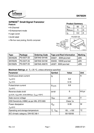
The SN7002N is an N‑channel enhancement‑mode, logic‑level small‑signal MOSFET offered in a PG‑SOT‑23 package. It is RoHS‑compliant, Pb‑free, and intended for low‑power switching applications.
The document lists maximum ratings, thermal characteristics, static and dynamic electrical parameters, safe operating area, and typical characteristic curves. Designers can use the provided values for drain current, breakdown voltage, on‑resistance, gate charge, and power dissipation when selecting the device for circuits.
| Continuous drain current (Id) at 25 °C | 0.2 A |
|---|---|
| Pulsed drain current (Id,puls) at 25 °C | 0.8 A |
| Power dissipation (P_R) at 25 °C | 0.36 W |
| Gate‑source voltage range (Vgs) | ±20 V |
| Drain‑source breakdown voltage (Vds) | 60 V |
| Gate threshold voltage (Vgs(th)) typical | 1.4 V |
| On‑state resistance (Rds(on)) typical | 3.9 Ω |
The device can conduct a continuous drain current of 0.2 A at 25 °C.
The SN7002N is rated for a drain‑source breakdown voltage of 60 V.
The allowed gate‑source voltage range is ±20 V.
The maximum power dissipation is 0.36 W at 25 °C.