
SPW52N50C3 is a high voltage MOS power transistor with the world's best RDS(on), ultra-low gate charge, periodic avalanche rating, extreme dv/dt rating, ultra-low effective capacitances and improved transconductance
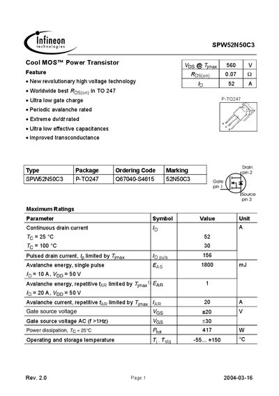
This datasheet describes the Infineon SPW52N50C3 Cool MOS power transistor, a 560 V, 52 A device in a P‑TO247 package. It lists key features such as ultra‑low gate charge, high voltage capability, and low on‑state resistance, together with detailed maximum ratings and thermal characteristics.
The document includes electrical parameters, transient thermal impedance, safe operating area curves, and typical output and transfer characteristics. It also provides packaging information, recommended operating temperature range, and legal notices from Infineon Technologies AG.
| Continuous drain current (Id) at 25 °C | 52 A |
|---|---|
| Pulsed drain current (Id) limited by Timax | 156 A |
| Avalanche energy, single pulse | 1800 mJ |
| Gate‑source voltage (DC) | +20 V |
| Gate‑source voltage (AC >1 Hz) | +30 V |
| Power dissipation at 25 °C | 417 W |
| Operating temperature range | -55 °C to +150 °C |
| Drain‑source breakdown voltage | 500 V |
| Input capacitance (Ciss) | 6800 pF |
The maximum continuous drain current is 52 A at a case temperature of 25 °C.
The single‑pulse avalanche energy is specified as 1800 mJ.
The device is rated for a DC gate‑source voltage of +20 V and an AC voltage of +30 V for frequencies above 1 Hz.
The transistor can operate from –55 °C up to +150 °C.