
This document describes the features and characteristics of the BSP89 SIPMOS small-signal transistor, including maximum voltage, drain current, power dissipation, operating temperature, etc.
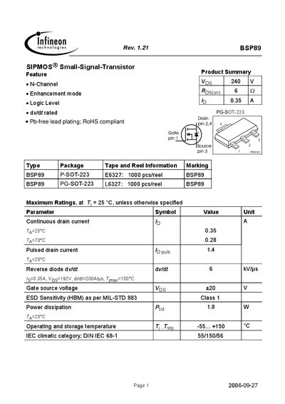
The BSP89 is an N‑channel enhancement‑mode small‑signal transistor offered in a P‑SOT‑223 package. The datasheet provides detailed electrical characteristics such as drain current limits, breakdown voltage, on‑state resistance and capacitances, as well as thermal parameters and safe operating area curves.
Packaging is supplied on tape and reel (1000 pcs/reel) and the component complies with RoHS and IEC climatic categories. The document also includes typical characteristic curves for output, transfer and gate charge behavior.
| Pulsed drain current (Id,pulse) | 1.4 A |
|---|---|
| Drain‑source breakdown voltage (Vds) | 240 V |
| On‑state resistance (Rds(on)) typ | 0.49 Ω |
| Power dissipation (Pd) | 1.8 W |
The device can handle a pulsed drain current of up to 1.4 A.
The drain‑source breakdown voltage is specified as 240 V.