
This document is a product summary of BSP297 Rev. 1.21 SIPMOS small-signal transistor. The transistor is an N-channel enhancement mode MOSFET with a maximum drain-source voltage of 200V and a drain-source on-resistance of 1.8Ω. Its features include enhancement mode logic level, dv/dt rating, and PG-SOT-223 package.
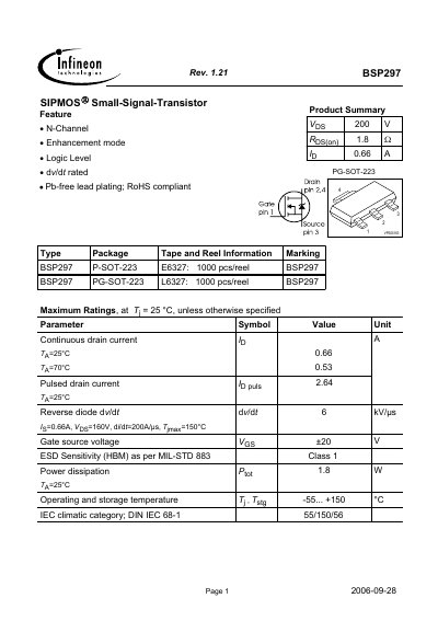
The BSP297 is an N‑channel enhancement‑mode, logic‑level small‑signal transistor offered in a PG‑SOT‑223 package. It is designed for low‑power and high‑frequency applications, featuring a maximum drain‑source voltage of 200 V and a continuous drain current of 0.66 A.
The document lists detailed electrical parameters such as on‑state resistance, gate threshold voltage, and capacitances, as well as thermal characteristics, power dissipation limits, and safe operating area curves. These specifications help designers assess suitability for their circuits and ensure reliable operation under the specified temperature ranges.
| Drain‑Source Breakdown Voltage (VDS) | 200 V |
|---|---|
| Continuous Drain Current (ID) | 0.66 A |
| On‑State Resistance (RDS(on)) | 1.2 Ω typ / 1.8 Ω max |
| Gate Threshold Voltage (VGS(th)) | 0.8 V typ – 1.8 V max |
| Power Dissipation (Ptot) | 1.8 W typ at 25 °C |
| Thermal Resistance Junction‑to‑Solder (RthJS) | 15 K/W typ – 25 K/W max |
| Thermal Resistance Junction‑to‑Ambient (RthJA) | 80 K/W typ – 115 K/W max |
The BSP297 can withstand a drain‑source voltage of up to 200 V.
The device is rated for a continuous drain current of 0.66 A.
The typical gate threshold voltage ranges from 0.8 V to 1.8 V.
It can dissipate about 1.8 W at 25 °C.