
Key facts
- Brand
- SYNC
- Model
- SPP3401
- Category
- MOS transistor
- Documents
- 2
- Languages
- EN
- Last added
- 2012-04-05
Start here
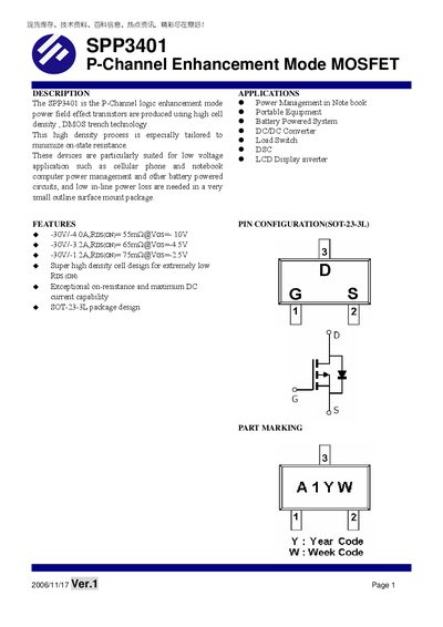
SYNC Power SPP3401 P-Channel MOSFET Datasheet
The SPP3401 is a P‑Channel logic enhancement mode MOSFET designed for low‑voltage power management in notebook computers, cellular phones, and other battery‑powered circuits. It uses a high‑density DMOS trench process to achieve very low on‑state resistance and compact SOT‑23‑3L packaging.
The datasheet provides absolute maximum ratings, electrical characteristics, typical transfer curves, and package dimensions, along with ordering information and a legal disclaimer from SYNC Power Corporation.
SYNC SPP3401 specifications
| Drain‑Source Voltage (V_DSS) | -30 V |
|---|---|
| Gate‑Source Voltage (V_GS) | +12 V |
| Continuous Drain Current (I_D) | -4.0 A |
| On‑Resistance (R_DS(on)) typical | 0.055 Ω |
| Power Dissipation (P_D) | 0.8 W |
| Thermal Resistance Junction‑to‑Ambient (RθJA) | 120 °C/W |
| Package | SOT‑23‑3L |
All SYNC SPP3401 documents by type
Ratings, dimensions and ordering codes, for selection and design work.
Questions answered in these manuals
What is the maximum drain‑source voltage rating?
The SPP3401 is rated for a maximum drain‑source voltage of -30 V.
Which package does the SPP3401 use?
It is supplied in a SOT‑23‑3L surface‑mount package.
What is the maximum drain‑source voltage of the SPP3401B?
The device is rated for a maximum drain‑source voltage of -30 V.
What is the typical on‑resistance of the SPP3401B?
Typical on‑resistance is about 0.080 Ω at V_GS = -4.5 V and I_D = -3.2 A.