
K5P2880YCM is a Multi ChipPackage Memory integrating 128Mbit Nand Flash and 8Mbit full CMOS SRAM produced by Samsung. It features single 3.0V power supply and supports 528-byte page program, 16K-byte block erase with 50ns reading speed.
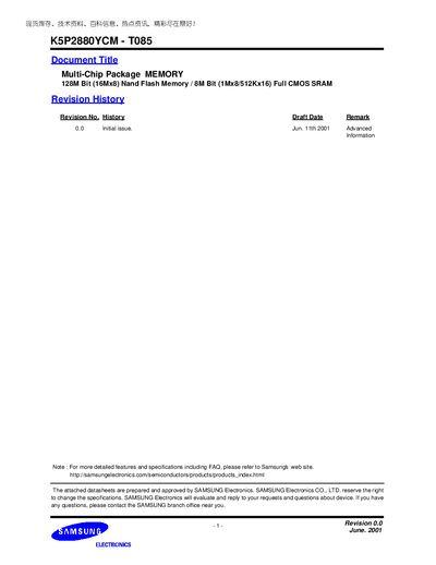
The K5P2880YCM - T085 is a multi‑chip package memory that combines a 128‑Mbit NAND flash and an 8‑Mbit full CMOS SRAM in a single 69‑ball TBGA package. It operates from a single 2.7 V to 3.3 V supply and is intended for mobile communication systems and other low‑power applications.
Key features include fast random access (10 µs max for flash), serial read of 50 ns, typical page program time of 300 µs, block erase time of 2 ms, 100 k program/erase endurance, and data retention of 10 years for flash and 1.5 V for SRAM. The device is packaged in a 8 × 13 mm, 0.8 mm pitch TBGA with 69 balls.
| Supply Voltage | 2.7 V to 3.3 V |
|---|---|
| Flash Organization | 16 M × 8 bit (128 Mbit) |
| SRAM Organization | 1 M × 8 bit or 512 K × 16 bit (8 Mbit) |
| Flash Random Access Time | 10 µs (max) |
| Flash Serial Read Time | 50 ns (min) |
| SRAM Access Time | 85 ns |
| Flash Read Current | 10 mA @20 MHz |
| Flash Program/Erase Current | 10 mA |
| Flash Standby Current | 10 pA |
| SRAM Operating Current | 20 mA |
| SRAM Standby Current | 0.5 pA |
| Page Program Size | 528 bytes (512 + 16) |
| Block Erase Size | 16 KB + 512 B |
| Typical Page Program Time | 300 µs |
| Typical Block Erase Time | 2 ms |
| Flash Endurance | 100 000 program/erase cycles (minimum) |
| Flash Data Retention | 10 years |
| SRAM Data Retention Voltage | 1.5 V (min) |
| Operating Temperature | -25 °C to 85 °C |
| Package | 69‑ball TBGA, 8 × 13 mm, 0.8 mm pitch |
It operates from 2.7 V to 3.3 V.
The flash can endure at least 100 000 program/erase cycles.
A typical page program takes about 300 µs.
It is supplied in a 69‑ball TBGA package measuring 8 × 13 mm with a 0.8 mm pitch.