
This document introduces the multi-chip package memory product of K5P2880YCM - T085 model from Dinghao. The product combines 128Mbit (16Mx8) Nand Flash Memory and 8Mbit (1Mx8/512Kx16) Full CMOS SRAM. The flash memory has fast programming and erasing performance, while the SRAM has high capacity and low power consumption.
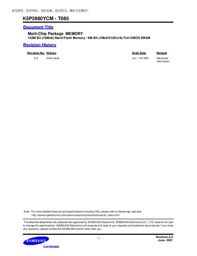
The K5P2880YCM is a multi‑chip package memory that combines a 128‑Mbit NAND flash with an 8‑Mbit full CMOS SRAM in a single 3.0 V powered device. It is intended for data memory in mobile communication systems, offering low power consumption and a compact 69‑ball TBGA package.
The datasheet provides electrical characteristics, timing diagrams, command sets, and package dimensions. Key specifications include a 2.7 V‑3.3 V supply range, 10 µs maximum random flash access, 50 ns minimum serial read, and a 100 k program/erase cycle endurance. Detailed pin descriptions and ball configurations are also included.
| Supply voltage | 2.7 V to 3.3 V |
|---|---|
| Flash random access time | 10 µs (max) |
| Flash serial read time | 50 ns (min) |
| SRAM access time | 85 ns |
| Flash read current | 10 mA @ 20 MHz |
| Flash program/erase current | 10 mA |
| Flash standby current | 10 pA |
| SRAM operating current | 20 mA |
| SRAM standby current | 0.5 pA |
| Flash endurance | 100,000 program/erase cycles (minimum) |
| Flash data retention | 10 years |
| SRAM data retention voltage | 1.5 V (min) |
| Operating temperature | -25 °C to 85 °C |
| Package | 69‑ball TBGA, 8 × 13 mm, 0.8 mm pitch |
It operates from 2.7 V up to 3.3 V.
The flash can endure at least 100,000 program/erase cycles.
The flash standby current is 10 pA.
It operates from –25 °C to 85 °C.