
TC7WBD125FK is a low on-resistance, high-speed CMOS 2-bit bus switch produced by TOSHIBA. It features typical CMOS characteristics: low power consumption and low propagation delay. When output enable (OE) is at low level, the switch is on; when at high level, the switch is off. The internal diode which adds to power supply line is enable to realize the shift of signal level from 5 V to 3.3 V.
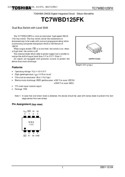
The TC7WBD125FK is a low‑on‑resistance, high‑speed CMOS dual‑bus switch with level‑shift capability, allowing connections or disconnections with minimal propagation delay and low power dissipation. When the output‑enable (OE) pin is low the switch is on; a high level turns it off. The device includes internal diodes for 5 V to 3.3 V level shifting and ESD protection on all inputs.
Key specifications include an operating voltage of 4.5‑5.5 V, typical on‑resistance of 5 Ω, propagation delay of 0.25 ns, and ESD ratings of +200 V (JEITA) and +2000 V (MIL). The part is supplied in an SSOP8‑P‑0.50A package and is intended for general electronics applications such as computers, office equipment, and industrial robotics.
| Operating voltage (Voc) | 4.5 ~ 5.5 V |
|---|---|
| Propagation delay (tpd) | 0.25 ns (max) |
| ESD performance | +200 V (JEITA), +2000 V (MIL) |
| Package | SSOP8‑P‑0.50A |
| Power dissipation (Pp) | 200 mW |
The device operates with a supply voltage (Voc) from 4.5 V to 5.5 V.
It meets ESD ratings of +200 V (JEITA) and +2000 V (MIL).
It is supplied in an SSOP8‑P‑0.50A surface‑mount package.