
Key facts
- Brand
- STMicroelectronics
- Model
- STP6NB50FP
- Documents
- 2
- Languages
- EN
- Last added
- 2012-04-01
Start here
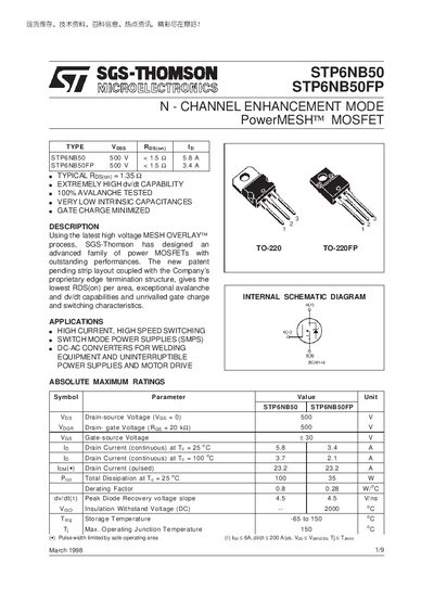
SGS-Thomson STP6NB50/FP Datasheet
This datasheet describes the STP6NB50 and STP6NB50FP power MOSFETs, highlighting their high‑voltage capability, low on‑resistance and fast switching performance. It includes absolute maximum ratings, typical electrical characteristics, and thermal data for both the TO‑220 and TO‑220FP packages.
Mechanical dimensions, thermal impedance curves, and gate‑charge characteristics are also presented, together with safety notices and corporate information. The document is intended for designers and engineers selecting MOSFETs for SMPS, welding converters, UPS and motor‑drive applications.
STMicroelectronics STP6NB50FP specifications
| Drain‑source voltage (VDS) | 500 V |
|---|---|
| Gate‑source voltage (VGS) | 30 V |
| Continuous drain current (ID) @ 25 °C | 5.8 A (STP6NB50) / 3.4 A (STP6NB50FP) |
| Total power dissipation @ 25 °C | 100 W (STP6NB50) / 35 W (STP6NB50FP) |
| Output capacitance (Coss) | 110 pF (typ) / 149 pF (max) |
| Junction‑case thermal resistance | 1.25 °C/W (STP6NB50) / 3.57 °C/W (STP6NB50FP) |
| Maximum lead temperature for soldering | 300 °C |
All STMicroelectronics STP6NB50FP documents by type
Ratings, dimensions and ordering codes, for selection and design work.
Questions answered in these manuals
What is the maximum drain‑source voltage rating?
The MOSFETs are rated for a maximum drain‑source voltage of 500 V.
How much continuous drain current can the STP6NB50 handle at 25 °C?
At 25 °C the STP6NB50 can conduct 5.8 A continuously (STP6NB50FP 3.4 A).
What is the maximum drain‑source voltage for the STP6NB50 and STP6NB50FP?
Both devices are rated for a maximum drain‑source voltage of 500 V.
What is the typical on‑resistance of the STP6NB50?
The typical RDS(on) for the STP6NB50 is 1.35 mΩ at VGS = 10 V.