
L6561 is the improved version of the L6560 standard Power Factor Corrector. Fully compatible with the standard version, it has a superior performing multiplier making the device capable of working in wide input voltage range applications (from 85V to 265V) with an excellent THD. Furthermore the start up current has been reduced at few tens of mA and a disable function has been implement- ed on the ZCD pin, guaranteeing lower current consumption in stand by mode. Realised in mixed BCD technology, the chip gives the following benefits: – micro power start up current – 1% precision internal reference voltage – (Tj = 25°C) – Soft Output Over Voltage Protection – no need for external low pass filter on the cur- rent sense – very low operating quiescent current minimis- es power dissipation The totem pole output stage is capable of driving a Power MOS or IGBT with source and sink cur- rents of ±400mA. The device is operating in tran- sition mode and it is optimised for Electronic Lamp Ballast application, AC-DC adaptors and SMPS.
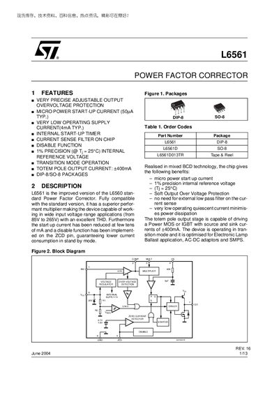
The L6561 is a Power Factor Corrector designed for a wide input voltage range (85 V to 265 V) and offers a precise adjustable output with built‑in over‑voltage protection. It features a very low quiescent supply current (4 mA typ.) and a micro‑power start‑up current of 50 µA typ., making it suitable for standby‑sensitive applications.
The device includes a totem‑pole output capable of driving MOSFETs or IGBTs with ±400 mA source and sink currents. Pin functions, absolute maximum ratings, and typical application circuits are detailed, along with evaluation results that demonstrate performance across the specified voltage range.
| Input voltage range | 85 V to 265 V |
|---|---|
| Output current (totem pole) | ±400 mA |
| Start‑up current | 50 µA typ. |
| Quiescent supply current | 4 mA typ. |
The L6561 operates from 85 V up to 265 V input voltage.
The totem‑pole output can source and sink up to ±400 mA.
Connecting the ZCD (Zero Current Detector) pin to ground disables the device.
The typical start‑up current is 50 µA.