
This document describes the features and characteristics of the AD9516-3, a 14-output clock generator with an integrated 2.0 GHz VCO. It includes low phase noise, phase-locked loop, reference inputs, output interfaces, etc.
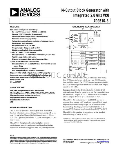
The AD9516-3 provides a multi‑output clock distribution function with sub‑picosecond jitter performance. It integrates a PLL and on‑chip VCO that tunes from 1.75 GHz to 2.25 GHz, and can also accept an external VCO/VCXO up to 2.4 GHz. The device supports a variety of reference inputs, programmable delays, and both digital and analog lock detection.
The part is offered in a 64‑lead LFCSP package, operates from a single 3.3 V supply, and delivers six LVPECL outputs (three pairs), four LVDS outputs (two pairs), and eight CMOS outputs. Output frequencies reach 2.95 GHz for LVPECL, 800 MHz for LVDS, and 250 MHz for CMOS, with configurable division ratios and fine‑delay adjustments.
| VCO Frequency Range (on‑chip) | 1.75 GHz – 2.25 GHz |
|---|---|
| Supply Voltage (Vs) | 3.135 V min – 3.3 V typ – 3.465 V max |
| Operating Temperature Range | ‑40 °C to +85 °C |
| Phase Noise @ 100 kHz Offset | ‑108 dBc/Hz |
The on‑chip VCO tunes from 1.75 GHz to 2.25 GHz.
It provides six LVPECL outputs arranged in three pairs.
The device operates from a 3.3 V supply, with a minimum of 3.135 V and a maximum of 3.465 V.
It is specified for operation from –40 °C to +85 °C.