
This document contains PCB footprint information for the SOT650-1 product, including pin size, pad size, solder area, etc.
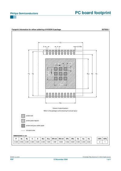
This document describes the PCB footprint for the Philips SOT650-1 HVSON10 package, including reflow soldering recommendations. It is intended for designers creating board layouts for this component.
The footprint follows a generic pattern with specific dimensions for pads, solder land, and solder paste deposit. All measurements are given in millimetres and reference the package outline drawing.
| Package type | HVSON10 |
|---|
The footprint follows the generic pattern and should be based on the package outline drawing provided in the manual.