
This document provides information on the PCB footprint and soldering dimensions for the SOT386-1 package from Philips Electronics.
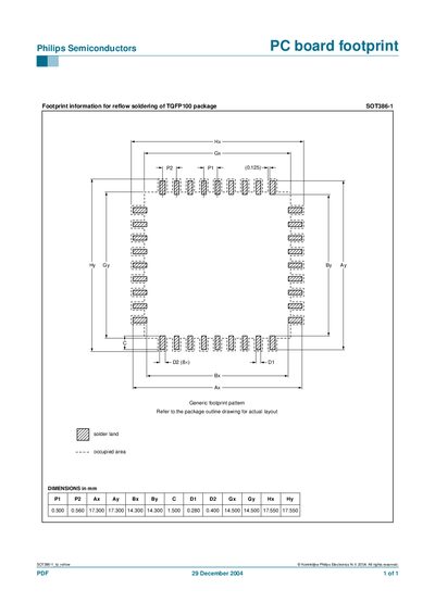
This document supplies the mechanical footprint information required for designing printed‑circuit‑board (PCB) layouts for the Philips SOT386-1 semiconductor package. It includes pad dimensions, spacing, and recommended reflow soldering parameters.
The footprint data are presented in millimetres, with key values such as pad pitch, pad size, and overall package dimensions. Users should refer to the package outline drawing for the exact layout before finalizing their PCB design.
| Pad pitch (P2) | 0.500 mm |
|---|---|
| Package width | 17.300 mm |
| Package height | 17.300 mm |
| Pad length (Ay) | 14.300 mm |
The footprint information is for the TQFP100 package SOT386-1.
The document was published in 2004.