
Provide PCB layout reference information for SOT589-1
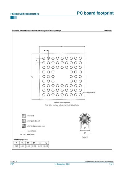
This document provides the PC‑board footprint details for the Philips SOT589-1 BGA553 package, including solder land, solder paste deposit, occupied area and solder resist guidelines. It is intended for designers performing reflow soldering.
The sheet lists the exact dimensions of the footprint (P, SL, sP, SR, Hx, Hy) in millimetres and refers to the package outline drawing for the actual layout. The information is copyrighted by Koninklijke Philips Eletronics N.V. (2004).
| P | 1.27 mm |
|---|---|
| SL | 0.600 mm |
| sP | 0.500 mm |
| SR | 0.750 mm |
| Hx | 38.075 mm |
| Hy | 38.075 mm |
It provides footprint information for reflow soldering, including solder land, solder paste deposit, occupied area and solder resist details.
Refer to the package outline drawing for the actual layout.
It was published on 14 September 2004.