
This document is about SOT617-1 PC board printed circuit design specification, including size, pad, pin information.
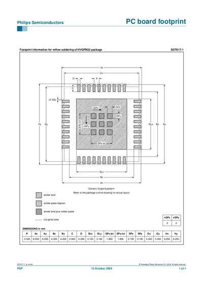
This document provides the printed‑circuit‑board (PCB) footprint data required for reflow soldering the Philips SOT617-1 HVQFN32 package. It lists the pad dimensions, spacing, and recommended solder‑paste deposition patterns.
A generic footprint pattern is shown, and the exact layout should be cross‑checked with the package outline drawing. All dimensions are given in millimetres.
| Package outline width | 6.250 mm |
|---|
The manual provides the exact pad dimensions, spacing and solder‑paste guidelines for the SOT617-1 HVQFN32 footprint.
The document advises to refer to the package outline drawing for the actual layout.
The guide shows a pattern of solder land plus solder paste for the footprint.