
This document is about the PCB board footprint dimensions of the SOT741-1_fp electronic component produced by Koninklijke Philips Electronics N.V. in 2004. The electronic component is a BGA376 package product suitable for reflow soldering. The document provides detailed information on the dimensions and solder pad layout of the electronic component.
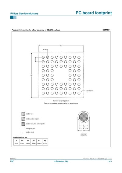
This document provides the PCB footprint information for the Philips SOT741-1 semiconductor device, which uses a BGA376 package. It includes details on solder land, solder paste deposit, and occupied area needed for reliable reflow soldering.
The generic footprint pattern dimensions are listed in millimetres, with pad length, width, solder resist, and overall package size. Refer to the package outline drawing for the exact layout.
| Pad length (SL) | 1.00 mm |
|---|---|
| Pad width (SP) | 0.450 mm |
| Solder resist width (SR) | 0.450 mm |
| Height (Hx) | 0.600 mm |
| Package width (Hy) | 23.575 mm |
The SOT741-1 uses the BGA376 package.
The generic footprint pattern has a pad length of 1.00 mm, pad width of 0.450 mm, solder resist width of 0.450 mm, height of 0.600 mm, and overall width of 23.575 mm.