
This document is about the dimensions of components on a PCB board, and it describes the features and characteristics of the SOT480-1 package.
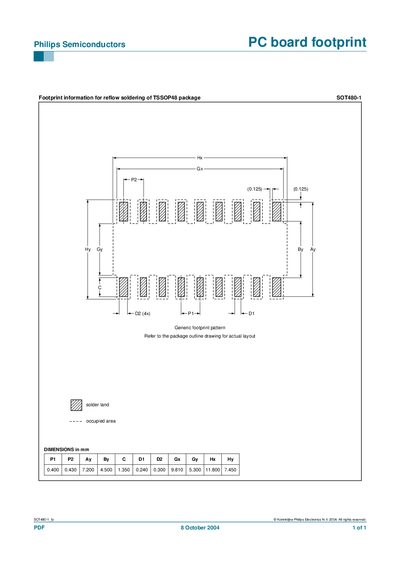
This manual gives the footprint information required for reflow soldering of the TSSOP48 SOT480-1 package. It includes a generic footprint pattern and references the package outline drawing for the exact layout.
The document lists all critical dimensions in millimetres, such as pad spacing, pad size, and overall footprint extents, enabling designers to create accurate PCB layouts for the component.
| P1 (pad length) | 0.400 mm |
|---|---|
| P2 (pad width) | 0.430 mm |
| Ay (pad centre‑to‑centre X) | 7.200 mm |
| By (pad centre‑to‑centre Y) | 4.500 mm |
| C (clearance) | 1.350 mm |
| D1 (solder land length) | 0.240 mm |
| D2 (solder land width) | 0.300 mm |
| Gx (overall width) | 9.810 mm |
| Gy (overall height) | 5.300 mm |
| Hx (overall length) | 11.800 mm |
| Hy (overall height) | 7.450 mm |
The manual provides a generic footprint pattern and lists all dimension values needed to create the PCB layout.
Pad length (P1) is 0.400 mm, pad width (P2) is 0.430 mm, with centre‑to‑centre spacing Ay = 7.200 mm and By = 4.500 mm.
The overall footprint measures Gx = 9.810 mm, Gy = 5.300 mm, Hx = 11.800 mm, and Hy = 7.450 mm.