
This document is about the PC board footprint of Philips Semiconductors from February 15, 2001. The document describes the soldering methods, solder lands, solder resist, and occupied area for SSOP, TSSOP, and VSO footprints.
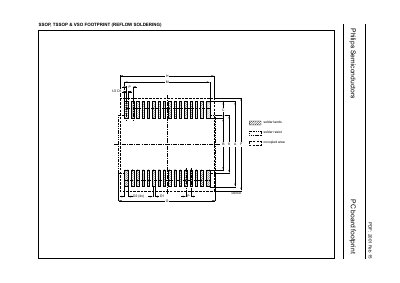
The document is a footprint handbook for Philips Semiconductors components. It lists the reflow‑soldering pad layouts and dimensions for SSOP, TSSOP and VSO package families.
A table on page 2 gives the outline code, package name, number of pins and key dimensions (length, width, lead pitch, etc.) together with placement accuracy tolerances for each variant.