
This document mainly introduces the PCB printed circuit board dimensions of SOT826-1, including Hx, Hy, P, SL, SP and SR parameters
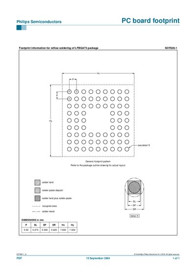
This manual supplies the PCB footprint information for the LFBGA73 package SOT826-1, intended for use in reflow soldering processes. It includes generic pattern guidelines and references to the package outline drawing for the actual layout.
The document lists the pad dimensions, solder land and paste specifications, occupied area, solder resist, and overall footprint dimensions in millimetres.
| Pad width (P) | 0.50 mm |
|---|---|
| Pad length (SL) | 0.275 mm |
| Solder mask opening (sP) | 0.300 mm |
| Solder mask opening (SR) | 0.425 mm |
| Footprint X dimension (Hx) | 7.500 mm |
| Footprint Y dimension (Hy) | 7.500 mm |
It covers the LFBGA73 package SOT826-1.
The footprint dimensions are P=0.50 mm, SL=0.275 mm, sP=0.300 mm, SR=0.425 mm, Hx=7.500 mm, Hy=7.500 mm.