
This application note shows recommendation device mount method & precaution for RD07&RD02 series.
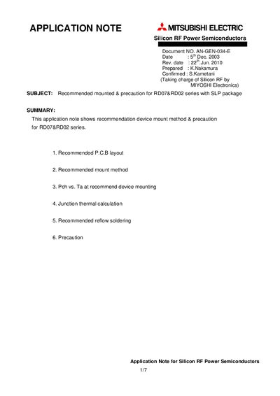
The document provides detailed recommendations for PCB layout, mounting methods, and reflow soldering profiles to ensure reliable operation of the RDO7 and RDO2 MOSFETs. It also includes thermal resistance values, junction temperature calculations, and guidelines to limit mechanical stress during assembly.
Key sections cover recommended PCB layout (regular triangle arrangement with 13 through‑holes), mount methods using heat‑sinks, thermal performance data (Rthj‑a values of 9.0 °C/W for RDO2 and 7.2 °C/W for RDO7), reflow soldering temperature profiles, and safety precautions for mobile‑communication versus base‑station use.
| Power dissipation capability | 11~14 W @ Ta=25 °C |
|---|---|
| Thermal resistance (Rthj‑a) – RDO2 | 9.0 °C/W |
| Thermal resistance (Rthj‑a) – RDO7 | 7.2 °C/W |
| Heat‑sink size (recommended) | 40.0 mm × 90.0 mm × 10.0 mm |
| Through‑hole plating thickness | 0.05 mm |
A regular triangle arrangement with 13 through‑holes and a plating thickness of 0.05 mm is recommended, with the source area on the underside of the board.
The operating junction temperature should be kept below 120 °C.