
XC74WL00AASR is a dual 2-input CMOS NAND gate, manufactured using silicon gate CMOS processes. The small supply current, which is one of the features of the CMOS logic, gives way to high speed operations which enables LS-TTL. With wave forming buffers connected internally, stabilized output can be achieved as the series offers high noise immunity. As the series is integrated into a mini molded, MSOP-8B package, high density mounting is possible.
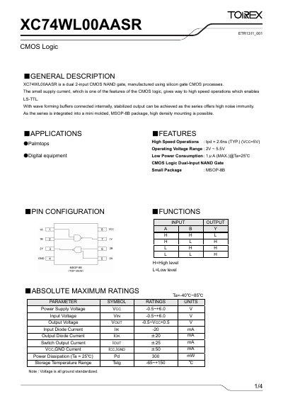
The XC74WL00AASR is a dual 2‑input CMOS NAND gate manufactured with silicon‑gate CMOS technology. It offers high‑speed operation, low power consumption, and a compact MSOP‑8B package suitable for portable and digital equipment.
The document lists pin assignments, absolute maximum ratings, recommended operating conditions, DC and switching electrical characteristics, as well as test circuit and waveform information for designers.
| Power Supply Voltage (VCC) | -0.5~+6.0 V |
|---|---|
| Input Voltage (VIN) | -0.5~+6.0 V |
| Output Voltage (VOUT) | -0.5~VCC+0.5 V |
| Propagation Delay (tpd) | 2.6 ns (typ) |
| Static Supply Current (ICC) | 1 µA (max) |
| Power Dissipation | 300 mW |
| Operating Temperature Range | -40 °C to +85 °C |
| Package | MSOP‑8B |
It is a dual 2‑input NAND gate.
The typical propagation delay is 2.6 ns at VCC = 5 V.
The recommended operating voltage range is 2 V to 5.5 V.
The device can dissipate up to 300 mW.