
The PI74SSTU32864A is a logic circuit produced by Pericom Semiconductor with SSTL_18 compatible inputs. The 25-bit 1:1 or 14-bit 1:2 configurable registered buffer is designed for operation at 1.7V to 1.9V VDD.
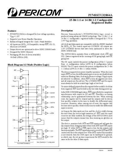
The PI74SSTU32864A is a 25‑Bit 1:1 or 14‑Bit 1:2 configurable registered buffer designed for low‑voltage operation (Vpp = 1.8 V) and DDR2 memory interfaces. All inputs are SSTL_18 compatible, while control inputs are LVCMOS, and the device supports low‑power standby mode.
The document includes detailed pin‑out tables for both 1:1 and 1:2 configurations, electrical and switching characteristics, maximum ratings, and mechanical packaging information for the 96‑ball LFBGA (NB) package. Ordering codes and test circuit examples are also provided.
| Supply Voltage (Vpp) | 1.8 V nominal |
|---|---|
| Maximum Clock Frequency | 270 MHz |
| Package Type | 96‑Ball LFBGA (NB) |
The device operates from a 1.8 V nominal Vpp supply.
The PI74SSTU32864A can operate up to 270 MHz.
It is supplied in a 96‑ball LFBGA (NB) package.
The buffer can be configured as a 25‑Bit 1:1 or a 14‑Bit 1:2 device.