
The document describes the features and characteristics of a product, including its functions, performance, and applications.
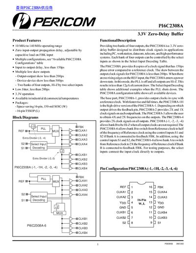
The PI6C2308A is a 3.3 V zero‑delay buffer that distributes clock signals with low jitter and skew. It offers two banks of four outputs, selectable configurations, and operates over a 10 MHz to 140 MHz frequency range.
The handbook contains product features, functional description, pin configuration, electrical and switching characteristics, operating conditions for commercial and industrial temperature ranges, package diagrams, and ordering information for the available SOIC and TSSOP packages.
| Operating frequency range | 10 MHz to 140 MHz |
|---|---|
| Input‑output propagation delay | < 150 ps |
| Output‑output skew | < 200 ps |
| Device‑device skew | < 500 ps |
| Supply voltage (Vpp) | 3.0 V – 3.6 V |
| Commercial operating temperature | 0 °C – 70 °C |
| Industrial operating temperature | -40 °C – 85 °C |
| Input LOW voltage | 0.8 V |
| Input HIGH voltage | 2.0 V |
| Load capacitance | 30 pF |
The device operates from 10 MHz up to 140 MHz.
It provides eight copies of the clock signal.
The part is offered in a 16‑pin 150‑mil SOIC (W) and a 16‑pin TSSOP (L) package.
The input‑output delay is less than 150 ps.