
The PI6C2408 is a PLL-based, zero-delay buffer, with the ability to distribute eight outputs of up to 140 MHz at 3.3 V. Two banks of four outputs exist, and, depending on product option ordered, can supply either reference frequency, prescaled half frequency, or multiplied 2x or 4x input clock frequencies.
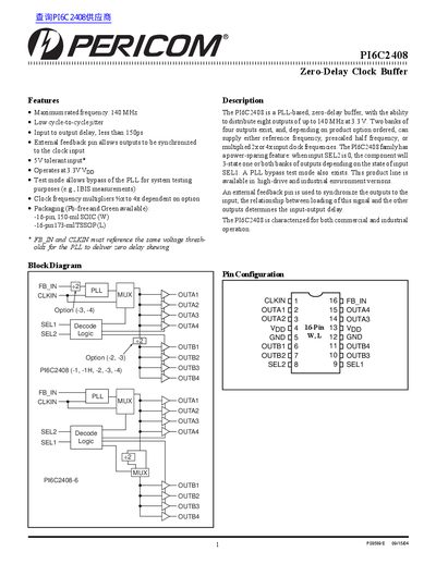
The PI6C2408 zero‑delay clock buffer distributes eight 140 MHz outputs at 3.3 V. It uses a PLL with an external feedback pin for synchronization, provides low cycle‑to‑cycle jitter, and includes a test mode that bypasses the PLL. Two banks of four outputs can be configured for reference, half‑frequency, or multiplied 2×/4× clock signals.
The device operates from –0.5 V to +7.0 V supply, is 5 V‑tolerant on inputs, and is offered in commercial and industrial temperature grades. Package options include 16‑pin 150‑mil SOIC (W) and 16‑pin 173‑mil TSSOP (L). Ordering codes differentiate temperature range and lead‑free/green versions.
| Maximum rated frequency | 140 MHz |
|---|---|
| Input‑to‑output delay | <150 ps |
| Operating voltage (VDD) | 3.3 V |
| Supply voltage range | –0.5 V to +7.0 V |
| Input tolerance | 5 V tolerant |
The device is rated for a maximum frequency of 140 MHz.
The input‑to‑output delay is less than 150 ps.
The buffer operates at 3.3 V VDD.