
Key facts
- Brand
- Linear Technology
- Model
- LTC6240
- Industry
- Industrial
- Documents
- 2
- Languages
- EN
- Last added
- 2012-05-09
Start here
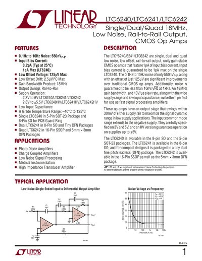
Linear Technology LTC6240/LTC6241/LTC6242 Datasheet
The LTC6240, LTC6241 and LTC6242 are low‑noise, low‑offset, rail‑to‑rail output CMOS op‑amps available in single, dual and quad configurations. They feature 1 pA input bias current (0.2 pA typical) and a gain‑bandwidth product of 18 MHz, making them suitable for high‑speed, low‑noise signal processing.
The document lists absolute maximum ratings, package and order information, detailed electrical characteristics, and typical application circuits such as photodiode amplifiers and low‑noise signal processing stages. Package options include SOT‑23, SO, DFN and SSOP with recommended solder pad layouts.
Linear Technology LTC6240 specifications
| Input Bias Current | 0.2 pA typ (1 pA max for LTC6240) |
|---|---|
| Input Offset Voltage | 125 µV max |
| Gain Bandwidth Product | 18 MHz |
| Slew Rate | 10 V/µs |
| Input Noise Voltage (0.1 Hz‑10 Hz) | 550 nV p‑p |
| Operating Temperature Range | ‑40 °C to 125 °C |
All Linear Technology LTC6240 documents by type
Ratings, dimensions and ordering codes, for selection and design work.
Questions answered in these manuals
What is the input bias current of the LTC6240?
The LTC6240 has an input bias current of 0.2 pA typical at 25 °C and a maximum of 1 pA.
What is the gain‑bandwidth product of the LTC6240/1/2?
All three devices have a gain‑bandwidth product of 18 MHz.
What is the typical noise voltage of the LTC6240 series?
The LTC6240/LTC6241/LTC6242 have a noise of 550 nVpp measured from 0.1 Hz to 10 Hz.
What supply voltage range does the LTC6240 operate over?
The standard LTC6240 operates from 2.8 V to 6 V, while the HV version operates up to 5.5 V.